Saturday, February 22, 2025
LTM15C458-11
Email: sales@shunlongwei.com
Website: https://www.slw-ele.com/ltm15c458-11.html
**Discover the LTM15C458-11 by Toshiba Matsushita – Your Ultimate Desktop Monitor Solution!**
**Key Product Specifications:**
- **Brand:** Toshiba Matsushita
- **Model P/N:** LTM15C458-11
- **Diagonal Size:** 15.0 inch
- **Panel Type:** a-Si TFT-LCD, LCM
- **Resolution:** 1024(RGB)×768, XGA 85PPI
- **Pixel Format:** RGB Vertical Stripe
- **Active Area:** 304.128(W)×228.096(H) mm
- **Bezel Opening:** 307.2(W)×231.2(H) mm
- **Outline Dimensions:** 331.6(W)×255(H)×13(D) mm
- **Luminance:** 350 cd/m² (Typ.)
- **Viewing Angle:** 80/80/80/70 (Typ.) (CR≥10), optimized for 6 o'clock viewing
- **Color Depth:** 16.2M, 72% NTSC
- **Mass:** 1.20Kgs (Typ.)
- **Refresh Rate:** 60Hz, with advanced options:
- 120Hz (60Hz Input): Embedded MEMC Circuit
- 120Hz+120Hz: 120Hz Panel + 120Hz Backlight
- 240Hz (60Hz Input): Embedded MEMC Circuit
- **Surface Treatment:** Antiglare, Hard coating (3H)
- **Contrast Ratio:** 450:1 (Typ.)
- **Work Mode:** TN, Normally White, Transmissive
- **Response Time:** 6/19 ms (Typ.) (Tr/Td)
- **Backlight:** 4 pcs CCFL, 50K hours lifespan, No Driver required
- **Usage:** Designed for Desktop Monitors
- **Touchscreen:** Without
- **Signal Type:** LVDS (1 ch, 8-bit), 20 pins Connector
- **Voltage Supply:** 3.3V (Typ.)
- **Max. Ratings:**
- Storage Temp.: -20 ~ 60 °C
- Operating Temp.: 0 ~ 50 °C
**Why Choose LTM15C458-11?**
With its high-quality TFT-LCD panel, excellent viewing angles, and advanced refresh rate options, this monitor delivers crisp visuals and smooth performance. Perfect for professional or personal use, it combines durability and precision in a compact design.
**Contact Us Today!**
Email: sales@shunlongwei.com
Visit: https://www.slw-ele.com/ltm15c458-11.html
Elevate your desktop experience with Toshiba Matsushita’s LTM15C458-11!
CM800DZB-34N
Email: sales@shunlongwei.com
Website: CM800DZB-34N
🚀 **Introducing the CM800DZB-34N – Your Ultimate Solution for High-Performance Connectivity!**
🔥 **What Makes It Stand Out?**
✔️ **Advanced Technology**: Designed with cutting-edge features for seamless integration.
✔️ **Reliability**: Built to deliver consistent performance in demanding environments.
✔️ **Versatility**: Perfect for a wide range of applications, from industrial to commercial use.
💡 **Why Choose Us?**
✅ **Expert Support**: Our team is here to guide you every step of the way.
✅ **Quality Assurance**: We ensure every product meets the highest standards.
✅ **Competitive Pricing**: Get top-tier technology without breaking the bank.
📩 **Ready to Elevate Your Connectivity Game?**
Contact us today at **sales@shunlongwei.com** to learn more about the CM800DZB-34N and how it can transform your operations!
#CM800DZB34N #ConnectivitySolutions #Innovation #Reliability #TechUpgrade
LP133X5-A2IB
Email: sales@shunlongwei.com
LP133X5-A2IB
Introducing the LP133X5-A2IB – your ultimate solution for cutting-edge display technology!
This high-performance display module is designed to deliver exceptional clarity, vibrant colors, and reliable functionality, making it the perfect choice for a wide range of applications.
Key Features:
✨ Crystal-clear visuals for an immersive experience
⚡ Energy-efficient design for sustainable performance
🛠️ Durable construction for long-lasting use
Whether you're upgrading your current setup or building a new project, the LP133X5-A2IB ensures top-tier quality and performance.
Contact us today to learn more or place your order!
📧 Email: sales@shunlongwei.com
🌐 Visit our website for more details.
#TechInnovation #DisplayTechnology #LP133X5A2IB #UpgradeYourExperience
7MBR30SA060E-01
{"choices":[{"message":{"content":"The **7MBR30SA060E-01** is a high-power IGBT (Insulated Gate Bipolar Transistor) module designed for industrial applications requiring robust voltage and current handling. Below is a structured breakdown of its key specifications and implications for use:\n\n---\n\n### **Absolute Maximum Ratings** \n1. **Voltage Ratings** \n - **Collector-Emitter Voltage (Vces):** 600V \n *Application:* Suitable for high-voltage circuits like inverters or motor drives. \n - **Gate-Emitter Voltage (VGES):** ±20V \n *Critical:* Gate driver circuitry must stay within this range to avoid damaging the oxide layer. \n\n2. **Current Ratings** \n - **Continuous Collector Current (Ic):** 30A @ Tc=25°C \n *Note:* Requires derating at higher case temperatures (check datasheet curves). \n - **Pulsed Collector Current (Icp):** 60A for 1ms @ Tc=25°C \n *Use Case:* Handles short overloads (e.g., motor startup). \n\n3. **Power and Thermal Limits** \n - **Power Dissipation (Pc):** 120W @ Tc=25°C \n *Thermal Design:* Heatsink required; power handling decreases with temperature. \n - **Junction Temperature (Tj):** +150°C (max operating limit). \n\n4. **Isolation and Safety** \n - **Isolation Voltage (VIsol):** 2500V AC (1 minute) \n *Purpose:* Ensures electrical isolation between module and heatsink for safety. \n\n5. **Mechanical** \n - **Mounting Torque:** 3.5 N·m \n *Importance:* Ensures proper thermal contact without damaging the package. \n\n6. **Temperature Range** \n - **Storage (Tstg):** -40°C to +125°C \n *Handling:* Avoid exposure beyond these limits during storage/transport. \n\n---\n\n### **Key Applications** \n- **Industrial Power Systems:** Motor drives, UPS, solar inverters, welding equipment. \n- **High-Voltage Switching:** Designed for 600V systems with transient surge tolerance. \n\n---\n\n### **Design Considerations** \n1. **Thermal Management** \n - Use a heatsink with low thermal resistance. \n - Monitor junction temperature to stay below 150°C. \n2. **Gate Driving** \n - Ensure gate voltage stays within ±20V (e.g., use gate driver ICs). \n3. **Derating** \n - Reduce current/power ratings at elevated temperatures (refer to derating curves). \n4. **Pulsed Currents** \n - Limit high-current pulses (60A) to ≤1ms to prevent overheating. \n\n---\n\n### **Part Number Interpretation** \nLikely breakdown: \n- **7MBR:** Series/family (e.g., 7th-gen IGBT module). \n- **30A:** Continuous current rating. \n- **SA060:** 600V voltage class. \n- **E-01:** Variant/revision. \n\n---\n\nThis module is ideal for demanding environments where high voltage, current, and reliability are critical. Proper adherence to ratings and thermal design ensures longevity and performance. Always consult the full datasheet for detailed derating and application guidelines.","reasoning_content":"Okay, so I need to understand the product details for this component called 7MBR30SA060E-01. Let me start by looking at the parameters provided. The first thing mentioned is Absolute Maximum Ratings at Tc=25°C unless otherwise specified. Absolute maximum ratings usually indicate the limits beyond which the device could be damaged, so these are critical values.\n\nThe first rating is Collector-Emitter voltage Vces: 600V. I remember that in transistors, the collector-emitter voltage is the maximum voltage that can be applied across the collector and emitter terminals without causing breakdown. So this device can handle up to 600V there. That's pretty high, so it's likely used in high-voltage applications.\n\nNext is Gate-Emitter voltage VGES: ±20V. For IGBTs or similar devices, the gate-emitter voltage is the voltage applied to turn the device on or off. The ±20V means that the gate can handle up to +20V and down to -20V. Exceeding this might damage the gate oxide layer. So the user must ensure the gate driver doesn't exceed these limits.\n\nCollector current Ic Continuous at Tc=25°C: 30A. This is the maximum continuous current the collector can handle when the case temperature is 25°C. But wait, in real applications, the case temperature might be higher, so the actual continuous current might be lower if the temperature rises. They might need to derate this current based on temperature.\n\nThen there's Collector current Icp 1ms Tc=25°C: 60A. This is the pulsed current, which can be higher for short durations. Here, it's 60A for 1 millisecond. So the device can handle short bursts of higher current, which is typical for switching applications where surges happen.\n\nCollector power dissipation Pc: 120W. This is the maximum power the device can dissipate. Power is calculated as V*I, so this would relate to thermal management. The device can handle 120W of power loss, but again, this is probably at Tc=25°C, and actual power handling would decrease as temperature increases.\n\nIsolation Voltage VIsol (AC 1 minute): 2500V. This is the isolation voltage between the device and the heatsink or mounting surface. It's tested with 2500V AC for one minute, meaning it can withstand that voltage without breakdown, ensuring safety and proper isolation in the system.\n\nOperating junction temperature Tj: +150°C. The maximum temperature the semiconductor junction can reach while operating. Staying below this is crucial for reliability. Thermal design must ensure the junction doesn't exceed this, considering ambient temperature, power dissipation, and thermal resistance.\n\nStorage temperature Tstg: -40 to +125°C. The temperature range where the device can be stored without damage. Even when not operating, it shouldn't be exposed to temperatures outside this range.\n\nMounting screw torque 3.5 *1 N·m. The torque applied when screwing the device to a heatsink. Proper torque ensures good thermal contact without damaging the package. Over-tightening can crack the device, under-tightening might lead to poor heat dissipation.\n\nNow, putting this all together, this seems like an IGBT module. The part number 7MBR30SA060E-01 might break down as follows: 7th generation, MBR maybe indicating a module type, 30A continuous current, SA could be series, 060 for 600V, E-01 version. But that's just a guess. The key specs are 600V, 30A continuous, 60A pulsed, 120W power dissipation, with high isolation voltage.\n\nIn applications, this would be used in power electronics like inverters, motor drives, or power supplies. The high voltage and current ratings suggest it's for industrial or heavy-duty applications. Thermal management is crucial here, as the power dissipation is significant, and the junction temperature must be kept under 150°C. The mounting torque is important for ensuring proper heat transfer to the heatsink. Also, the isolation voltage is necessary for safety in systems where the module is attached to a grounded heatsink but operates at high potentials.\n\nPotential considerations when using this device: need a heatsink with adequate thermal performance, proper gate driving circuitry that stays within ±20V, ensuring that operating conditions don't exceed the absolute maximum ratings, especially under transient conditions. Derating currents and power dissipation at higher temperatures would be necessary. For example, if the case temperature is higher than 25°C, the continuous current rating would decrease. The user must refer to the derating curves in the datasheet for accurate values.\n\nAlso, the 1ms pulsed current of 60A suggests that it can handle short overloads, which is common in motor starting or fault conditions. But the duration is critical; exceeding 1ms might cause overheating. The isolation voltage ensures that there's no electrical leakage between the module and the mounting surface, which is vital for user safety and system integrity.\n\nIn summary, this component is a high-power IGBT module suited for switching high voltages and currents in demanding environments. Proper attention to thermal design, voltage and current limits, and mechanical mounting is essential for reliable operation.","role":"assistant"},"finish_reason":"stop","index":0,"logprobs":null}],"object":"chat.completion","usage":{"prompt_tokens":158,"completion_tokens":1798,"total_tokens":1956},"created":1740223046,"system_fingerprint":null,"model":"deepseek-r1","id":"chatcmpl-f594ca60-30d2-99a4-af94-d08983e82cf3"}
Thursday, February 20, 2025


 https://www.slw-ele.com/wp-content/uploads/2025/02/IMG_0006-1.jpg
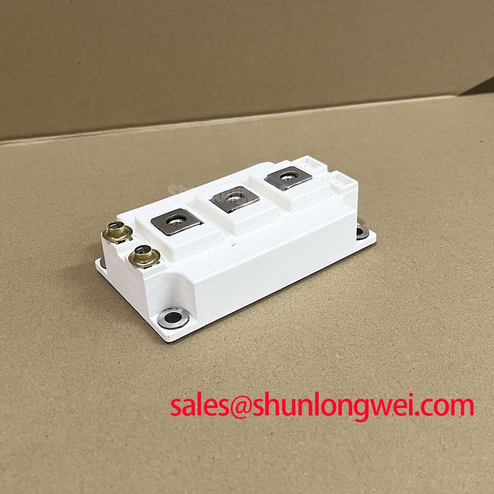
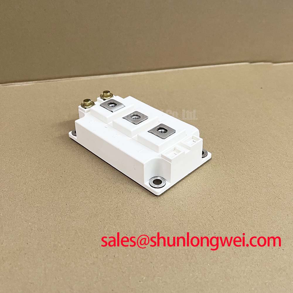
MMG400D060B6EN
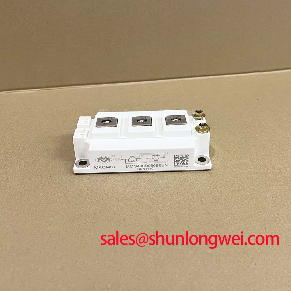

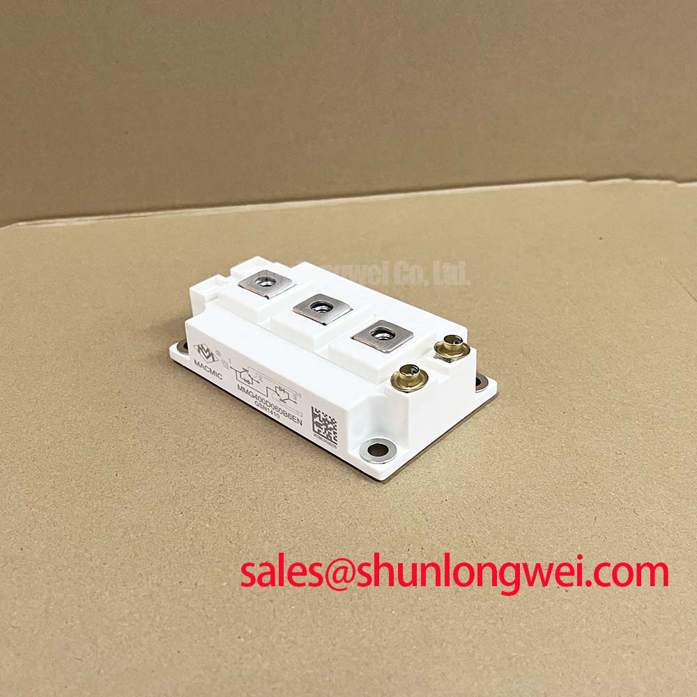


 PRODUCTFEATURES
IGBT² CHIP(Trench+Field Stop technology)
High short circuit capability,self limiting short circuit current
VcE(sat)with positive temperature coefficient
Fast switching and short tail current
Free wheeling diodes with fast and soft reverse recovery
Low switching losses
APPLICATIONS
High frequency switching application
Medical applications
Motion/servo control
UPS systems
IGBT-inverter
ABSOLUTE MAXIMUM RATINGS Tc=25°C unless otherwise specified
VCES Collector-Emitter Voltage 600V
VGES Gate-Emitter voltage:±20V
±lc Collector Current Tc= 25°C 400A
±ICP Collector Current (Peak) TC= 25°C 800A
PC Collector Dissipation TC= 25°C 1250W
Tj Junction Temperature -40~+150°C
Tstg Storage Temperature -40~+125°C
Viso Isolation Voltage 60Hz, Sinusoidal, Charged part to Base, AC 1 min. 3000V
Mounting screw torque M6 2.5~5 N·m
Weight 300g
https://www.slw-ele.com/wp-content/uploads/2025/02/IMG_0012-1.jpg
PRODUCTFEATURES
IGBT² CHIP(Trench+Field Stop technology)
High short circuit capability,self limiting short circuit current
VcE(sat)with positive temperature coefficient
Fast switching and short tail current
Free wheeling diodes with fast and soft reverse recovery
Low switching losses
APPLICATIONS
High frequency switching application
Medical applications
Motion/servo control
UPS systems
IGBT-inverter
ABSOLUTE MAXIMUM RATINGS Tc=25°C unless otherwise specified
VCES Collector-Emitter Voltage 600V
VGES Gate-Emitter voltage:±20V
±lc Collector Current Tc= 25°C 400A
±ICP Collector Current (Peak) TC= 25°C 800A
PC Collector Dissipation TC= 25°C 1250W
Tj Junction Temperature -40~+150°C
Tstg Storage Temperature -40~+125°C
Viso Isolation Voltage 60Hz, Sinusoidal, Charged part to Base, AC 1 min. 3000V
Mounting screw torque M6 2.5~5 N·m
Weight 300g
https://www.slw-ele.com/wp-content/uploads/2025/02/IMG_0012-1.jpg
MI-J20-IY/S
sales@shunlongwei.com https://www.slw-ele.com/mi-j20-iy-s.html
Check out our latest product features! Up to 90% efficiency, single output 2 – 48Vdc, MIL-STD-810 environments, and more. Perfect for your high-performance needs. Visit our website for details. #Electronics #PowerConverter #Innovation
Subscribe to:
Posts (Atom)